Introduction
Here, we create the memory modules for the computer.
Basic chips
Bit
In order to create blocks of memory, we first need to be able to store just one bit of information: a zero or a one. This is done by using a D Flip-Flop (Data Flip-Flop). The flip-flop on its own can store a single bit, but it is not complete yet. We need to be able to choose whether (and when) to keep the current bit, or store (load) a new bit.
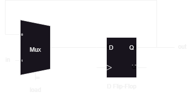
The above diagram shows a circuit which allows us to choose to keep the current bit or load a new one.
D is the input to the D Flip-Flop and Q is the output. The other two inputs for the D Flip-Flop are not used.
When load=0 the current bit is kept by feeding the output Q into the multiplexer, which feeds back into the input of the flip-flop.
When load=1 the in bit is fed into the input of the flip-flop, thus loading a new bit.
CHIP Bit {
    IN in, load;
    OUT out;

    PARTS:
    Mux (a=DFFo, b=in, sel=load, out=m);
    DFF (in=m, out=DFFo, out=out);
}
Register
A register is simply a battery of multiple bits. Registers are just a small amount of memory, typically between 8-bits and 64-bits. In this case, the register is 16-bits wide.
Note (out of interest):
-
A
Nibbleis 4-bits -
A
Byteis 8-bits -
A
WORDis 16-bits -
A
DWORD(double word) is 32-bits -
A
QWORD(quadruple word) is 64-bits
So our 16-bit register is called a WORD.
CHIP Register {
    IN in[16], load;
    OUT out[16];

    PARTS:
    Bit (in=in[0],  load=load, out=out[0]);
    Bit (in=in[1],  load=load, out=out[1]);
    Bit (in=in[2],  load=load, out=out[2]);
    Bit (in=in[3],  load=load, out=out[3]);
    Bit (in=in[4],  load=load, out=out[4]);
    Bit (in=in[5],  load=load, out=out[5]);
    Bit (in=in[6],  load=load, out=out[6]);
    Bit (in=in[7],  load=load, out=out[7]);
    Bit (in=in[8],  load=load, out=out[8]);
    Bit (in=in[9],  load=load, out=out[9]);
    Bit (in=in[10], load=load, out=out[10]);
    Bit (in=in[11], load=load, out=out[11]);
    Bit (in=in[12], load=load, out=out[12]);
    Bit (in=in[13], load=load, out=out[13]);
    Bit (in=in[14], load=load, out=out[14]);
    Bit (in=in[15], load=load, out=out[15]);
}
Program Counter (PC)
With RAM, we can have kilobytes, megabytes, and even gigabytes of memory. If you imagine RAM to be a book, then a computer (you) may want to access page 432 of a book and read 10 pages of it, then go to page 862 and read 50 pages from the book. While people can just read the page number and know which page to go to next, computers need a little help.
A “program counter” is a special piece of memory which does just that. It stores the current memory address (the page) and can increment that address to get the next piece of memory (the next page). It can also load a new address (go to a different page) and continue reading from there.
We can accomplish this digitally by using a “pipeline” approach shown in the image below (note that all inputs/outputs are 16-bits wide, and the select/load bits are just 1-bit wide).
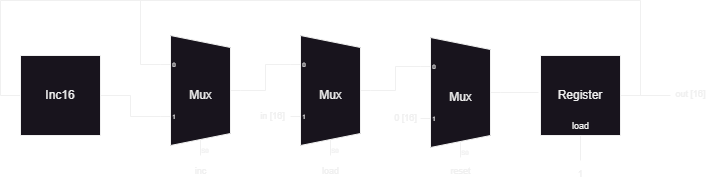
Each multiplexer represents a stage at which we can manipulate the program counter. We can choose whether to increment the current memory address (inc), whether load a new address (load), and whether to set the memory address to 0 (reset). In the end, the result is stored in a register.
CHIP PC {
    IN in[16],load,inc,reset;
    OUT out[16];

    PARTS:
    Inc16 (in=reg, out=incr);

    Mux16 (a=reg, b=incr,  sel=inc,   out=m0);
    Mux16 (a=m0,  b=in,    sel=load,  out=m1);
    Mux16 (a=m1,  b=false, sel=reset, out=m2);

    Register (in=m2, load=true, out=reg, out=out);
}
Random Access Memory (RAM)
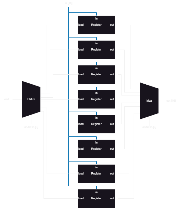
RAM8
Here we have eight registers that need to be accessed individually. If we need to load a register, we can use a demultiplexer to choose which register to load. If we need to read a register, we can use a multiplexer to choose which register to output.
CHIP RAM8 {
    IN in[16], load, address[3];
    OUT out[16];

    PARTS:
    DMux8Way (in=load, sel=address, a=ld0, b=ld1, c=ld2, d=ld3, e=ld4, f=ld5, g=ld6, h=ld7);
    Register (in=in, load=ld0, out=o0);
    Register (in=in, load=ld1, out=o1);
    Register (in=in, load=ld2, out=o2);
    Register (in=in, load=ld3, out=o3);
    Register (in=in, load=ld4, out=o4);
    Register (in=in, load=ld5, out=o5);
    Register (in=in, load=ld6, out=o6);
    Register (in=in, load=ld7, out=o7);
    Mux8Way16 (a=o0, b=o1, c=o2, d=o3, e=o4, f=o5, g=o6, h=o7, sel=address, out=out);
}
RAM64
The RAM64 module is similar to RAM8. It should be noted that the multiplexer and demultiplexer use the most-significant-bits (MSB), while the addresses use the least-significant-bits (LSB). This is because the MSB chooses which RAM8 modules to access, while the LSB chooses the smaller RAM modules (the registers) in RAM8. A similar concept applies to all the other RAM modules made in this project.
CHIP RAM64 {
IN in[16], load, address[6];
OUT out[16];
PARTS:
DMux8Way (in=load, sel=address[3..5], a=ld0, b=ld1, c=ld2, d=ld3, e=ld4, f=ld5, g=ld6, h=ld7);
RAM8 (in=in, address=address[0..2], load=ld0, out=o0);
RAM8 (in=in, address=address[0..2], load=ld1, out=o1);
RAM8 (in=in, address=address[0..2], load=ld2, out=o2);
RAM8 (in=in, address=address[0..2], load=ld3, out=o3);
RAM8 (in=in, address=address[0..2], load=ld4, out=o4);
RAM8 (in=in, address=address[0..2], load=ld5, out=o5);
RAM8 (in=in, address=address[0..2], load=ld6, out=o6);
RAM8 (in=in, address=address[0..2], load=ld7, out=o7);
Mux8Way16 (a=o0, b=o1, c=o2, d=o3, e=o4, f=o5, g=o6, h=o7, sel=address[3..5], out=out);
}RAM512
CHIP RAM512 {
IN in[16], load, address[9];
OUT out[16];
PARTS:
DMux8Way (in=load, sel=address[6..8], a=ld0, b=ld1, c=ld2, d=ld3, e=ld4, f=ld5, g=ld6, h=ld7);
RAM64 (in=in, address=address[0..5], load=ld0, out=o0);
RAM64 (in=in, address=address[0..5], load=ld1, out=o1);
RAM64 (in=in, address=address[0..5], load=ld2, out=o2);
RAM64 (in=in, address=address[0..5], load=ld3, out=o3);
RAM64 (in=in, address=address[0..5], load=ld4, out=o4);
RAM64 (in=in, address=address[0..5], load=ld5, out=o5);
RAM64 (in=in, address=address[0..5], load=ld6, out=o6);
RAM64 (in=in, address=address[0..5], load=ld7, out=o7);
Mux8Way16 (a=o0, b=o1, c=o2, d=o3, e=o4, f=o5, g=o6, h=o7, sel=address[6..8], out=out);
}RAM4k
CHIP RAM4K {
    IN in[16], load, address[12];
    OUT out[16];

    PARTS:
    DMux8Way (in=load, sel=address[9..11], a=ld0, b=ld1, c=ld2, d=ld3, e=ld4, f=ld5, g=ld6, h=ld7);
    RAM512 (in=in, address=address[0..8], load=ld0, out=o0);
    RAM512 (in=in, address=address[0..8], load=ld1, out=o1);
    RAM512 (in=in, address=address[0..8], load=ld2, out=o2);
    RAM512 (in=in, address=address[0..8], load=ld3, out=o3);
    RAM512 (in=in, address=address[0..8], load=ld4, out=o4);
    RAM512 (in=in, address=address[0..8], load=ld5, out=o5);
    RAM512 (in=in, address=address[0..8], load=ld6, out=o6);
    RAM512 (in=in, address=address[0..8], load=ld7, out=o7);
    Mux8Way16 (a=o0, b=o1, c=o2, d=o3, e=o4, f=o5, g=o6, h=o7, sel=address[9..11], out=out);
}
RAM16k
This one is a little different from the previous RAM modules. All the other RAM modules went up by a factor of eight (8, 64, 512, 4k). but this module only goes up by a factor of four (4k to 16k). Thus, instead of using DMux8Way and Mux8Way16, we use DMux4Way and Mux4Way16.
CHIP RAM16K {
IN in[16], load, address[14];
OUT out[16];
PARTS:
DMux4Way (in=load, sel=address[12..13], a=ld0, b=ld1, c=ld2, d=ld3);
RAM4K (in=in, address=address[0..11], load=ld0, out=o0);
RAM4K (in=in, address=address[0..11], load=ld1, out=o1);
RAM4K (in=in, address=address[0..11], load=ld2, out=o2);
RAM4K (in=in, address=address[0..11], load=ld3, out=o3);
Mux4Way16 (a=o0, b=o1, c=o2, d=o3, sel=address[12..13], out=out);
}