
Introduction
In an effort to design a simple computer from the ground up, we need to create the relevant hardware to make such a machine work. The logic chips used in this course, and built in this post, are the foundation for this simple computer and the proceeding course projects.
The Canonical Logic Gates
All boolean logic can be represented using three logic operators: NOT, AND, and OR. If only these three operators are used, then the boolean expression is said to be in Canonical Form. In this project, we are only provided with a NAND gate, but with just this gate, we can build the three basic logic operators.
| A | B | OUT |
|---|---|---|
| 0 | 0 | 1 |
| 0 | 1 | 1 |
| 1 | 0 | 1 |
| 1 | 1 | 0 |
The NAND gate takes two inputs. Only when the both inputs are true is the output false.
NOT gate
The NOT gate (inverter) has the following truth table:
| IN | OUT |
|---|---|
| 0 | 1 |
| 1 | 0 |
That is, the input bit is simply inverted.
Since we have only been provided with NAND gates, we must somehow make a NOT gate from a NAND gate. But a NOT gate only takes a single input, while a NAND gate has two inputs. To solve this, if we look at the truth table of a NAND gate (Table 1), we notice that when A=B=0, that the output is 1. And when A=B=1, the output is 0. So, we simply connect the inputs together and a NOT gate is formed!
Here’s a schematic of a NAND gate connected to become a NOT gate:
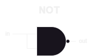
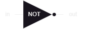
And the following image shows how a NOT gate is represented in schematics:
The code below is the implementation of a NOT gate using a NAND gate.
CHIP Not {
    IN in;
    OUT out;

    PARTS:
    Nand (a=in, b=in, out=out);

}
AND gate
Creating an AND gate is fairly simple once we have an inverter. Looking at the AND gate truth table, we can see that the output is similar to the output of a NAND gate, just inverted. NAND, in fact, stands for “NOT AND”.
| A | B | OUT |
|---|---|---|
| 0 | 0 | 0 |
| 0 | 1 | 0 |
| 1 | 0 | 0 |
| 1 | 1 | 1 |
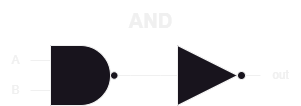
Below is a schematic version of the implementation
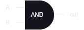
And below is how an AND gate is normally represented in schematics
And finally the HDL implementation
CHIP And {
IN a, b;
OUT out;

    PARTS:
    Nand (a=a, b=b, out=y1);
    Not  (in=y1, out=out);

}
OR gate
The OR gate has the following truth table
| A | B | OUT |
|---|---|---|
| 0 | 0 | 0 |
| 0 | 1 | 1 |
| 1 | 0 | 1 |
| 1 | 1 | 1 |
The OR gate sets its output to true when either A or B or both are true. This may seem a bit odd as this isn’t how we use “or” linguistically, but just accept it for now.
The implementation of an OR gate is more interesting than the previous gates. To implement this gate, we can make use of De Morgan’s Theorem.
Note that
- ∧ means logical AND
- ∨ means logical OR
- means logical NOT (in this case, NOT x)
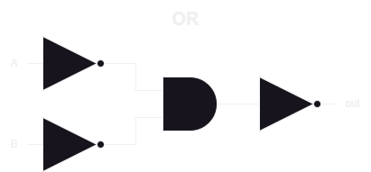
De Morgan’s theorem reads as (NOT A) AND (NOT B) = NOT (A OR B).
Now, a problem with this is that it gives us an inverted OR as the output (called a NOR gate). So we must invert the output to get just an OR gate.
The above boolean equation is demonstrated by the schematic below
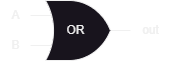
The normal schematic representation of an OR gate is shown below
And finally the pertaining code
CHIP Or {
IN a, b;
OUT out;

    PARTS:
    Not (in=a, out=n1);
    Not (in=b, out=n2);
    And (a=n1, b=n2, out=a1);
    Not (in=a1, out=out);

}
Another Logic Gate and Chips
We make one more logic gate, and two logic “chips” here.
- The XOR gate. It wasn’t lumped with the previous gates as it wasn’t canonical.
- The multiplexer. It isn’t a logic gate, but instead just a circuit that is built from logic gates.
- The demultiplexer, which is the complement of the multiplexer.
Exclusive OR (XOR) gate
The XOR gate is what we linguistically think of when we say “or”. Just like in the movie The Matrix, when Morpheus offers Neo the Red or Blue pill, he may only take one pill but not both (unlike an OR gate).
An XOR gate, which stands for “eXclusive OR”, is much the same way: we may choose one option or the other, but not both. The following is the truth table for an XOR gate.
| A | B | OUT |
|---|---|---|
| 0 | 0 | 0 |
| 0 | 1 | 1 |
| 1 | 0 | 1 |
| 1 | 1 | 0 |
The XOR gate is sometimes called a “Difference Gate”, as the output is only true when both inputs are different from each other. Out of interest, if we invert the output we get an XNOR gate, which is sometimes called an “Equality Gate”, as the output is only true when both inputs are the same.
To create an XOR gate, we can create a boolean expression by examining when the output is true.
We then can take the expression and implement it using previous logic gates. The colouring is for clarity and has nothing to do with Neo and Morpheus 😄
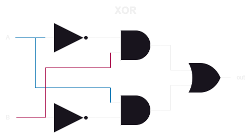
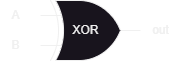
As usual, the schematic representation
And finally the code
CHIP Xor {
IN a, b;
OUT out;

    PARTS:
    Not (in=a, out=n1);
    Not (in=b, out=n2);
    And (a=a,  b=n2, out=a1);
    And (a=n1, b=b,  out=a2);
    Or  (a=a1, b=a2, out=out);

}
Multiplexer (MUX)
A multiplexer routes either A or B to the output, depending on the sel (select) bit.
| A | B | sel | OUT |
|---|---|---|---|
| 0 | 0 | 0 | A |
| 0 | 1 | 1 | B |
| 1 | 0 | 1 | B |
| 1 | 1 | 0 | A |
Notice that the output is written as A or B and not a number. This is because we only care about what input we route to the output, and not the input’s actual value. When sel=0 then OUT=A, and when sel=1 then OUT=B. Seeing the schematic makes the logic a lot easier to understand.
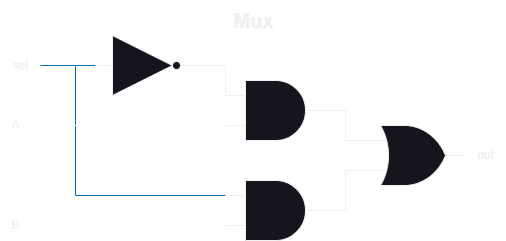
Since we already know about AND, OR, and NOT, then the logic should be fairly easy to follow along, but an example follows:
- Set
sel=0(expected output is A) - Examine two conditions: When
A=0andA=1 - When
A=0- The top AND gate sees
sel(which equals1), andA=0, therefore… - …the top AND gate outputs
0 - The bottom AND gate sees
sel=0so it outputs0 - The OR gate sees two zero inputs and therefore outputs
0, which is the value ofA
- The top AND gate sees
- When
A=1- The top AND gate sees
sel(which equals1), andA=1, therefore… - …the top AND gate outputs
1 - The bottom AND gate sees
sel=0so it outputs0 - The OR gate sees
1and0on its inputs and therefore outputs1, which is the value ofA
- The top AND gate sees
If we want to output B, just set sel=1.
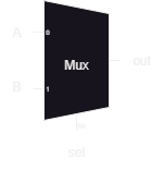
Below is the schematic representation usually seen for MUX “chips”.
And the code
CHIP Mux {
IN a, b, sel;
OUT out;

    PARTS:
    Not (in=sel, out=nsel);

    And (a=a, b=nsel, out=a1);
    And (a=b, b=sel,  out=a2);

    Or (a=a1, b=a2, out=out);

}
Demultiplexer (DMUX)
Compared to the multiplexer, the demultiplexer is a bit more complicated. While the multiplexer routes multiple inputs to one output, the demultiplexer routes one input to multiple outputs.
| in | sel | A | B |
|---|---|---|---|
| 0 | 0 | in | 0 |
| 0 | 1 | 0 | in |
| 1 | 0 | in | 0 |
| 1 | 1 | 0 | in |
Similar to the multiplexer, our two outputs have either 0 or in. The input itself isn’t important, just which output it has been routed to. When sel=0 then A=in, and when sel=1 then B=in.
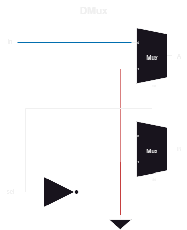
The implementation above uses two multiplexers. Let’s walk through an example
- Set
sel=0. The expected output isA. - The top multiplexer selects input “0” (the blue line going into the top multiplexer).
The input is routed to output A (
A=in) - The bottom multiplexer sees
sel(which equals 1). - The bottom multiplexer selects input “1” (the red line going into the bottom multiplexer).
This input is attached to
GND(ground), which is logic 0. The output isB=0.
When sel=1, the opposite happens.
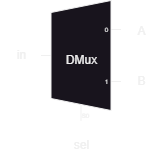
CHIP DMux {
IN in, sel;
OUT a, b;

    PARTS:
    Not (in=sel, out=nsel);
    Mux (a=in, b=false, sel=sel,  out=a);
    Mux (a=in, b=false, sel=nsel, out=b);
}
Multi-bit Gates and Chips
The first few multi-bit gates are rather easy and don’t require much explanation
Not16
This is just a bank of 16 individual NOT gates
CHIP Not16 {
IN in[16];
OUT out[16];

    PARTS:
    Not (in=in[0],  out=out[0]);
    Not (in=in[1],  out=out[1]);
    Not (in=in[2],  out=out[2]);
    Not (in=in[3],  out=out[3]);
    Not (in=in[4],  out=out[4]);
    Not (in=in[5],  out=out[5]);
    Not (in=in[6],  out=out[6]);
    Not (in=in[7],  out=out[7]);
    Not (in=in[8],  out=out[8]);
    Not (in=in[9],  out=out[9]);
    Not (in=in[10], out=out[10]);
    Not (in=in[11], out=out[11]);
    Not (in=in[12], out=out[12]);
    Not (in=in[13], out=out[13]);
    Not (in=in[14], out=out[14]);
    Not (in=in[15], out=out[15]);
}
And16
This is just a bank of 16 individual AND gates
CHIP And16 {
IN a[16], b[16];
OUT out[16];

    PARTS:
    And (a=a[0],  b=b[0],  out=out[0]);
    And (a=a[1],  b=b[1],  out=out[1]);
    And (a=a[2],  b=b[2],  out=out[2]);
    And (a=a[3],  b=b[3],  out=out[3]);
    And (a=a[4],  b=b[4],  out=out[4]);
    And (a=a[5],  b=b[5],  out=out[5]);
    And (a=a[6],  b=b[6],  out=out[6]);
    And (a=a[7],  b=b[7],  out=out[7]);
    And (a=a[8],  b=b[8],  out=out[8]);
    And (a=a[9],  b=b[9],  out=out[9]);
    And (a=a[10], b=b[10], out=out[10]);
    And (a=a[11], b=b[11], out=out[11]);
    And (a=a[12], b=b[12], out=out[12]);
    And (a=a[13], b=b[13], out=out[13]);
    And (a=a[14], b=b[14], out=out[14]);
    And (a=a[15], b=b[15], out=out[15]);
}
Or16
This is just a bank of 16 individual OR gates
CHIP Or16 {
IN a[16], b[16];
OUT out[16];

    PARTS:
    Or (a=a[0],  b=b[0],  out=out[0]);
    Or (a=a[1],  b=b[1],  out=out[1]);
    Or (a=a[2],  b=b[2],  out=out[2]);
    Or (a=a[3],  b=b[3],  out=out[3]);
    Or (a=a[4],  b=b[4],  out=out[4]);
    Or (a=a[5],  b=b[5],  out=out[5]);
    Or (a=a[6],  b=b[6],  out=out[6]);
    Or (a=a[7],  b=b[7],  out=out[7]);
    Or (a=a[8],  b=b[8],  out=out[8]);
    Or (a=a[9],  b=b[9],  out=out[9]);
    Or (a=a[10], b=b[10], out=out[10]);
    Or (a=a[11], b=b[11], out=out[11]);
    Or (a=a[12], b=b[12], out=out[12]);
    Or (a=a[13], b=b[13], out=out[13]);
    Or (a=a[14], b=b[14], out=out[14]);
    Or (a=a[15], b=b[15], out=out[15]);
}
Mux16
This a just a bank of 16 multiplexers. All of them are controlled simultaneously by a single sel bit
CHIP Mux16 {
IN a[16], b[16], sel;
OUT out[16];

    PARTS:
    Mux (a=a[0],  b=b[0],  sel=sel, out=out[0]);
    Mux (a=a[1],  b=b[1],  sel=sel, out=out[1]);
    Mux (a=a[2],  b=b[2],  sel=sel, out=out[2]);
    Mux (a=a[3],  b=b[3],  sel=sel, out=out[3]);
    Mux (a=a[4],  b=b[4],  sel=sel, out=out[4]);
    Mux (a=a[5],  b=b[5],  sel=sel, out=out[5]);
    Mux (a=a[6],  b=b[6],  sel=sel, out=out[6]);
    Mux (a=a[7],  b=b[7],  sel=sel, out=out[7]);
    Mux (a=a[8],  b=b[8],  sel=sel, out=out[8]);
    Mux (a=a[9],  b=b[9],  sel=sel, out=out[9]);
    Mux (a=a[10], b=b[10], sel=sel, out=out[10]);
    Mux (a=a[11], b=b[11], sel=sel, out=out[11]);
    Mux (a=a[12], b=b[12], sel=sel, out=out[12]);
    Mux (a=a[13], b=b[13], sel=sel, out=out[13]);
    Mux (a=a[14], b=b[14], sel=sel, out=out[14]);
    Mux (a=a[15], b=b[15], sel=sel, out=out[15]);
}
Mux4Way16
Mux4Way16 takes four 16-bit inputs and routes it to a single 16-bit output. There are two select bits, sel[0] and sel[1].
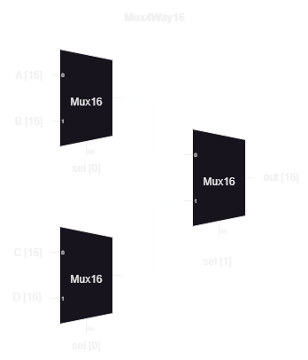
If sel[0]=0 then A is chosen from the top multiplexer and C is chosen from the bottom multiplexer.
If sel[0]=1 then B is chosen from the top multiplexer and D is chosen from the bottom multiplexer.
From there, sel[1] selects which of the two preceding multiplexers to use. For example, if sel[1]=0 then the top multiplexer would be used.
CHIP Mux4Way16 {
IN a[16], b[16], c[16], d[16], sel[2];
OUT out[16];

    PARTS:
    Mux16 (a=a,  b=b,  sel=sel[0], out=m1);
    Mux16 (a=c,  b=d,  sel=sel[0], out=m2);
    Mux16 (a=m1, b=m2, sel=sel[1], out=out);
}
Mux8Way16
Mux8Way16 has a similar construct to the preceding Mux4Way16. We just replace two of the Mux16 with Mux4Way16 instead.
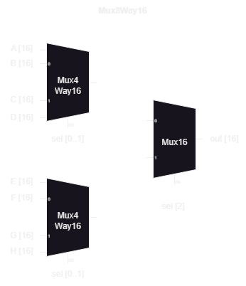
CHIP Mux8Way16 {
IN a[16], b[16], c[16], d[16],
e[16], f[16], g[16], h[16],
sel[3];
OUT out[16];

    PARTS:
    Mux4Way16 (a=a, b=b, c=c, d=d, sel=sel[0..1], out=m1);
    Mux4Way16 (a=e, b=f, c=g, d=h, sel=sel[0..1], out=m2);
    Mux16 (a=m1, b=m2, sel=sel[2] , out=out);
}
DMux4Way
The DMux4Way is essentially the Mux4Way16, but backwards and using demultiplexers. Note that the DMux4Way isn’t 16-bit.
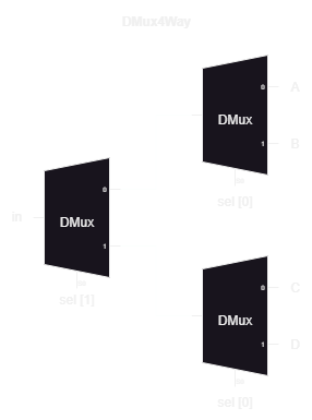
CHIP DMux4Way {
IN in, sel[2];
OUT a, b, c, d;

    PARTS:
    DMux (in=in, sel=sel[1], a=d1, b=d2);
    DMux (in=d1, sel=sel[0], a=a,  b=b);
    DMux (in=d2, sel=sel[0], a=c,  b=d);
}
DMux8Way
After the previous circuits, this requires no explanation. Just note that this also isn’t 16-bit.
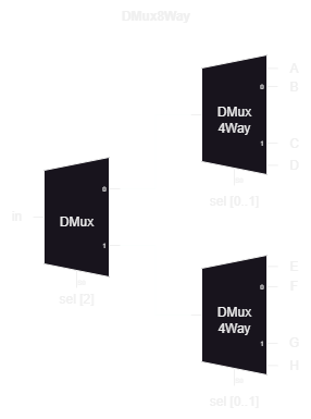
CHIP DMux8Way {
IN in, sel[3];
OUT a, b, c, d, e, f, g, h;

    PARTS:
    DMux (in=in, sel=sel[2], a=o1, b=o2);
    DMux4Way (in=o1, sel=sel[0..1], a=a, b=b, c=c, d=d);
    DMux4Way (in=o2, sel=sel[0..1], a=e, b=f, c=g, d=h);
}
Or8Way
Or8Way is the final multi-bit chip. It ORs eight bits together to produce a single output. Implementing this requires cascading seven OR gates together, feeding the output of one OR gate, into the input of another.
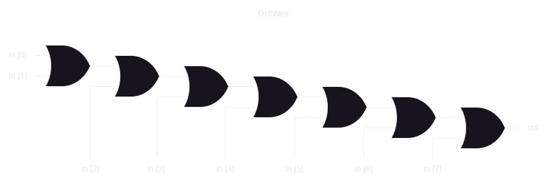
CHIP Or8Way {
IN in[8];
OUT out;

    PARTS:
    Or (a=in[0], b=in[1], out=o1);
    Or (a=in[2], b=o1,    out=o2);
    Or (a=in[3], b=o2,    out=o3);
    Or (a=in[4], b=o3,    out=o4);
    Or (a=in[5], b=o4,    out=o5);
    Or (a=in[6], b=o5,    out=o6);
    Or (a=in[7], b=o6,    out=out);
}